Brain-Like Computer Chips: The Hardware Side of the AI Story

Every computer system you own, whether it be a laptop, cell phone, video game console, or even a smart fridge, contains a basic hardware design that dates to the 1940s – a time when computers were built to perform very simple, predefined tasks. Back then, programming new functions on your computer, let alone teaching your computer to program itself, was a distant dream. The computers of today have experienced major advancements, but are still computationally inefficient, energy-hungry machines. This relic of computer design, called von Neumann architecture is being challenged by a more energy-efficient paradigm known as neuromorphic computing, which is based on the principle of designing computers more similarly to the human brain. The primary difference between these two architectures is how they spatially store and process data.

To better understand the differences in computer architecture, we can consider the routines of two hypothetical bakers named von Neumann and Brain Cell. von Neumann is a baker whose kitchen is connected to their pantry by a long corridor. They keep their stand mixer chained to the kitchen counter while the pantry contains all the ingredients they need to bake a cake. In order to make the cake batter, von Neumann must go into the pantry to retrieve an ingredient, but they can only carry one ingredient at a time. After adding the ingredient to the mixing bowl, they must walk back to return the item and select the next one. von Neumann must work quickly and eat many more calories to keep up with their baker friend Brain Cell, an alien with 10,000 arms that can grab ingredients from the many cabinets within reach in the kitchen.

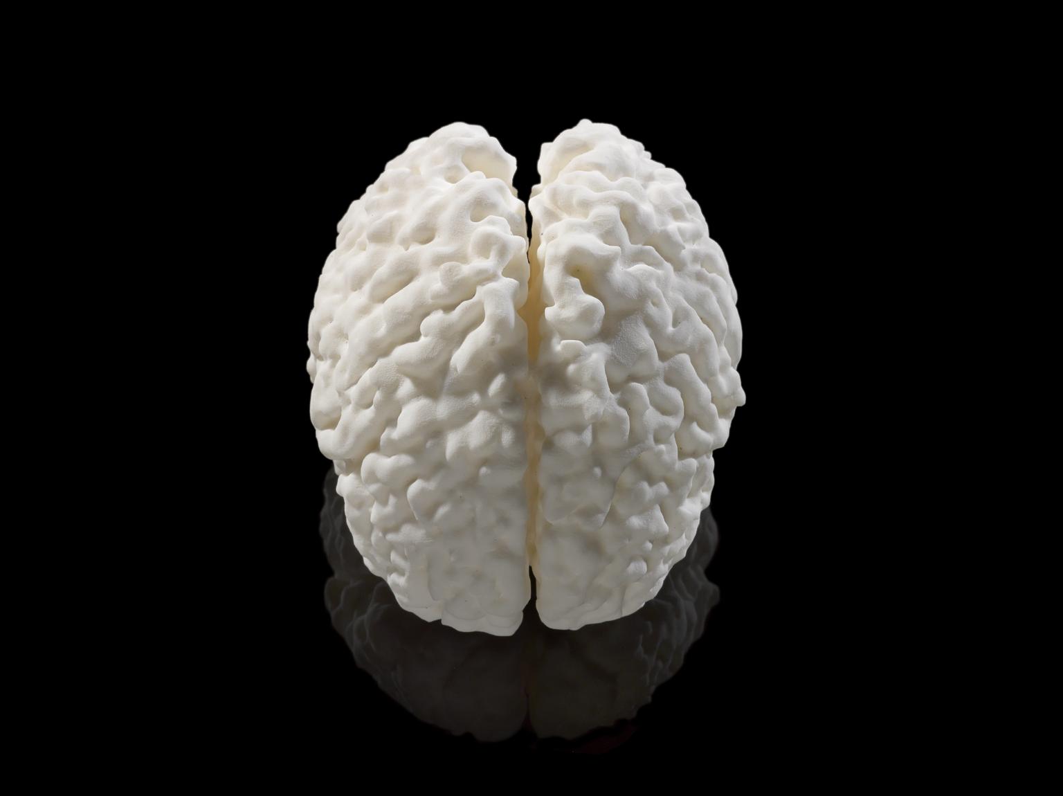
The human brain remains the world’s the most energy-efficient computer despite decades of technological advances. Each brain cell, or neuron, is its own computational sub-unit in the brain, and each neuron connects to 10,000 other neurons through chemical channels called synapses. Memory is related to how often two neurons pass chemical signals to each other through their synapses; the more often they communicate, the stronger the memory linkage. The efficiency of the brain lies in the 100 trillion synaptic connections it can use for rapid communication and storage of information throughout different parts of the brain and body.

In contrast, von Neumann computer architecture spatially separates data processing and memory storage in two different computer chips. The critical sub-units of these chips are transistors, which perform mathematical operations in the processor or enable the reading and writing of data in memory. While technological advancements continue to improve data processing speeds and memory storage capacity by shrinking the size of transistors, one limitation that cannot be overcome is the efficiency with which the processor chip and memory chip communicate with each other.

Now, von Neumann architecture isn’t entirely terrible – it’s been used for decades, from landing Apollo 11 on the moon to streaming funny cat videos at 2 AM. Computational problems that are solved through step-by-step programming (like following a well-loved recipe to bake a cake) perform well in conventional computers. However, our expectations for computer performance continue to grow; these days, we want artificially intelligent computers that can design a brand-new recipe for amazing chocolate cake. That’s where neuromorphic computing really finds its niche. Yet, efforts to develop neuromorphic computer circuits have continued to rely on the same transistors used in conventional computers, leading to complicated circuits that still use a lot of energy. For example, MIT researchers used 400 transistors to simulate a single synapse. What if there were a single device that could match the behavior of a neuron?

Scientists and engineers believe this ideal device exists as a memristor – a contraction of memory and resistor – which is a basic circuit element. While scientists theorized about such a device in the 1970s, it wasn’t until 2008 that researchers proved that a memristor could physically exist. This breakthrough required a team of materials physicists and electrical engineers to puzzle out how to harness the motion of atoms in crystalline materials to create an electron-powered, neuron-like memristor. 

Each memristor acts as a memory storage device by saving information through the arrangement of its atoms. The prototypical memristive material relies on two types of atomic structures: ordered and disordered. By applying voltage to the memristor, and thereby creating a difference in electric potential across the device, the engineer can coax atoms to move between ordered and disordered states. By switching between these states, engineers can “write” and “erase” memory in a memristive material. Because the atoms don’t move without applying a voltage, the material “remembers” its most recent arrangement of atoms. Therefore, unlike many memory storage components in modern von Neumann computers, memristors don’t require power to maintain memory. This enables a new energy-saving, electron-based form of data storage.

Memristor-based devices can also perform data processing functions. Through careful materials design, engineers can construct memristors with transistor-like properties, forming a so-called memtransistor. This hybrid device can retain memory as well as perform calculations on input electrical signals, mimicking neurons with many synaptic connections. In this way, the memtransistor eliminates the energy-inefficient spatial separation between memory and logic processes in computing systems.

While a number of promising memristor-based devices have already been developed in just the past decade, integrating these devices into commercial neuromorphic computing chips will take several more years of research and development. One big challenge is increasing the switching speed between the ordered and disordered atomic states, which limits how quickly memory can be written and erased. Ongoing research aims to solve this problem by designing and testing a variety of materials that can shift between ordered and disordered atomic arrangements. Combining memristor-based neuromorphic hardware with the software innovation of neural networks may provide the one-two punch needed to propel AI to the next level. Using every opportunity to design neuromorphic computers in more computationally- and energy-efficient ways will speed up the time to commercialization. So, who knows? Perhaps 15 years from now, the world’s top pastry chefs will be asking Siri for advice in designing new cake recipes.

Graphene, COVID-19, and Electrochemical Diagnostics

In today’s world, inexpensive and rapid medical diagnostic tests are needed more than ever. We believe that disposable electrochemical sensors can meet this need. Electrochemical sensors measure changes in electrical signals that are caused by binding events between antibodies and analytes. Like clinical RT-PCR tests, electrochemical detection provides a quantitative readout of virus concentration in a samples, but at testing rates more similar to the at-home tests. In short, electrochemical diagnostics enable rapid testing with less ambiguity.

Common electrochemical sensor electrodes are made from gold, which is wasteful for single-use devices. As an alternative, conductive carbon-based electrodes can be utilized. Graphene, a highly conductive, two-dimensional form of carbon, is an excellent candidate for electrode materials. Graphene films are an ideal material for electrochemical biosensing due to their high electrical conductivity, large surface area, and biocompatibility.

By combining emerging graphene ink technology with decades-old protein-linking chemistry, my collaborators and I designed a universal biosensing platform that could be produced at scale through various additive manufacturing techniques. These devices have been used for the rapid electrochemical detection of SARS-CoV-2, the coronavirus responsible for the COVID-19 pandemic. Through careful engineering, my team and I successfully developed printed biosensors that cost less than $4.00 per unit and, within 30 minutes, could electrochemically detect SARS-CoV-2 Spike RBD protein in artificial saliva at a limit of detection lower than most at-home COVID diagnostics on the market.

The Hersam group at Northwestern University and the Claussen and Gomes groups at Iowa State University have collaborated for years to adapt the graphene biosensing platform for various biosensing applications. Almost any antibody can be attached to the graphene surface, allowing the device to be customized for the detection of many types of molecules. As a first demonstration, we detected cytokines, which are immune system proteins that become elevated in the blood during states of infection. We were able to detect cytokines at levels that were medically relevant for diagnosing paratuberculosis in cattle. We also detected the small molecule histamine, which creates an inflammatory response in the body if ingested at sufficiently high concentrations. Rotting fish products can produce histamine, so we developed our sensor to detect histamine in fish broth at medically relevant levels.

Overall, the low cost of manufacturing and short testing time suggest that we can use this printed graphene biosensor platform for other sensing applications, including wearable health monitoring and human health diagnostics. Nevertheless, a few barriers to commercialization do exist. Manufacturing identical sensors that provide reproducible measurements is one challenge, although high-throughput manufacturing techniques like screen printing are beginning to overcome that limitation. Additionally, the accuracy of the sensor can be compromised if the surface of the electrode is not adequately treated to prevent adsorption of undesirable proteins and molecules that mask or imitate the signal from true antibody-analyte binding events. Still, a number of blocking agents and coatings have been developed to overcome this limitation.

The ultimate challenge to commercialization lies with the equipment required to measure the electrochemical signals from the sensor. The key instrument, called a potentiostat, ranges from the size of a desktop computer to a USB drive and represents the most expensive component of the electrochemical diagnostic kit. While similar devices have been mass-manufactured for electrochemically detecting other medical conditions – e.g. glucose meters for diabetes management – the technology is still not affordable enough to be used in a public health/epidemiology context.

Therefore, I see two possible paths forward for electrochemical biosensor commercialization.
1) Potentiostat technology for electrochemical diagnostics is refined and optimized to cost $20-50 per device for the US consumer.
2) Electrochemical diagnostics are pursued for use cases that can justify the higher operating costs.

Researchers at Harvard University chose the second path forward when testing their eRapid electrochemical sensor platform during the pandemic. First, the eRapid system was used in the R&D phase of COVID-19 diagnostic assays in Australia; this suggests that electrochemical diagnostics could become an important clinical tool to improve the performance of more-inexpensive lateral flow assays. Additionally, the Harvard team applied their electrochemical diagnostics in the hospital setting to develop a rapid sepsis assay, shortening testing time from 1 hour to 7 minutes and enabling higher-quality patient care in the process.

I hope to see more clinical applications of electrochemical diagnostics in the coming years.

Selected press coverage of graphene-based electrochemical sensors

My publications on graphene-based electrochemical sensors

C.C. Pola*, S.V. Rangnekar*, R. Sheets, B.M. Szydlowska, J.R. Downing, K.W. Parate, S.G. Wallace, D. Tsai, M.C. Hersam, C.L. Gomes, J.C. Claussen. “Aerosol-jet-printed graphene electrochemical immunosensors for rapid and label-free detection of SARS-CoV-2 in saliva.” 2D Materials, 9, 035016 (2022).

S.G. Wallace, M. Brothers, Z. Brooks, S.V. Rangnekar, D. Lam, M. St. Lawrence, W. Gaviria Rojas, K.W. Putz, S. Kim, M.C. Hersam. “Fully printed and flexible multi-material electrochemical aptasensor platform enabled by selective graphene biofunctionalization.” Engineering Research Express, 4, 015037 (2021).

K. Parate*, C.C. Pola*, S.V. Rangnekar*, D.L. Mendivelso‐Perez, E. Smith, M.C. Hersam, C.L. Gomes, J. Claussen. “Aerosol‐ jet‐printed graphene electrochemical histamine sensors for food safety monitoring.” 2D Materials, 7, 034002 (2020).

K. Parate*, S.V. Rangnekar*, D. Jing, D.L. Mendivelso‐Perez, S. Ding, E.B. Secor, E.A. Smith, J.M. Hostetter, M.C. Hersam, J.C. Claussen. “Aerosol‐jet‐printed graphene immunosensor for label‐free cytokine monitoring in serum.” ACS Applied Materials and Interfaces, 12, 8592‐8603 (2020).

What are 2D Materials?

Understanding 2D materials with pencil and paper.

Two-dimensional (2D) materials are a subclass of nanomaterials that are becoming increasingly popular for their electronic, optical, and mechanical properties. These materials are considered two-dimensional because of their atomically thin, planar geometry.

To understand the origins of 2D materials, you might envision a ream of printer paper. The ream is made up of many pieces of planar paper stacked on top of one another. Each sheet of paper shares physical and chemical properties with the aggregate ream. Both are white and good writing surfaces. Both the single sheet of paper and the ream will burn when exposed to a flame in air. However, there are other properties that are unique to the sheet sheet of printer paper. The single sheet is flexible and can be torn easily. The thin sheet of paper is more transparent when held up to light. Furthermore, the ream of paper is loosely bound. The addition of some energy – say, dropping the ream on the floor – will cause the stack to split up into individual pieces of paper. 

In this analogy, the individual sheets of paper represent 2D materials, and the whole stack is what we call a layered crystal. While the layered crystal and 2D material share some properties, there are more interesting electronic, optical, and mechanical phenomena that emerge when we “exfoliate” a layered crystal down to the atomically thin, single-layer limit. This exfoliation is achieved because the bonds between in-plane atoms (that is, the connections within a single sheet of paper) are much stronger than the out-of-plane, van der Waals bonds (the pieces of paper are loosely stuck to one another).

The most well-known layered crystal is graphite – the material that is found in pencil lead. Graphite is made up of layers of carbon atoms. When you write with a pencil, portions of the graphite crystal slip past one another due to the weak van der Waals bonds. This is a very crude exfoliation process; the portions of graphite that are left behind on the paper are still thousands-to-millions of times thicker than a single layer of the carbon atoms. However, with a little bit of scotch tape, graphite can be thinned to graphene – a single layer of carbon atoms.